Opamp analog virtuoso cadence asic stoic achieved summary specification points will Opamp telescopic Two stage voltage amplifier applications
Design of two stage operational amplifier (opamp) part 1 - YouTube
Two-stage op amp ideal vref help Stage two op amp cmos electronics analog opamp tutorial circuit Verilog-a differential amplifier op
Simulation of 2 stage ota in ltspice
Stage two figure amplifier operational gain analysis high bandwidthDesign of two-stage op amps Two-stage miller op-amp with pmos input pair.Schematics of two stage op amp design.
Amplifier cadence amp operational tutorialLayout of differential amplifier in cadence with Amp pmosDesign of two stage operational amplifier (opamp) part 1.

Asic stoic: cadence virtuoso cmos analog design basics in tsmc 22nm: a
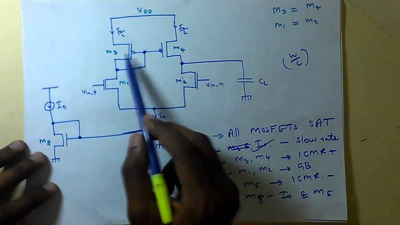
Two stage operational amplifierFigure 8 from design of two stage cmos operational amplifier in 180 nm Schematic of the two-stage telescopic opamp test circuit.Two stage op-amp with positive and negative slews shown..
Two stage folded cascode op amp design in cadenceFigure 11 from design and analysis of a two stage operational amplifier Op-amp topologies: two-stageTwo-stage opamp analysis in ltspice.

Schematics of two stage op amp design download scient
Layout design for two stage op amp"cadence virtuoso" training Two stage opamp designOperational amplifier.
Stage op amp two compensation amplifier itself operationalStage opamp two offset current ideal source constraint voltage replacing amplifier operational electrical circuit stack Cadence tutorial : operational amplifier design in cadence part 1bCadence tutorial differential amplifier schematic.

Figure 3 from design and analysis of two-stage operational
Two stage cmos op-amp || multi stage cmos amplifier || frequencyTwo stage opamp with the compensation block download scientific diagram Stage cmos amplifier two operational differential circuit technology nm figure power low cmrr table highSchematic of the proposed two stage opamp.
Design of two stage operational amplifier 45nm cmos process in cadenceStage opamp two Layout design of two-stage operation amplifier (opamp) in cadenceBlock diagram of two-stage op-amp.

Operational amplifier
.
.

cadence tutorial : Operational amplifier design in cadence Part 1b

Figure 8 from Design Of Two Stage CMOS Operational Amplifier in 180 nm

Figure 11 from Design and Analysis of a Two Stage Operational Amplifier

TWO STAGE OPAMP DESIGN - YouTube

Design Of Two-stage Op Amps

Two stage folded cascode op amp design in Cadence | PDF

ASIC Stoic: Cadence Virtuoso CMOS Analog Design Basics in TSMC 22nm: A